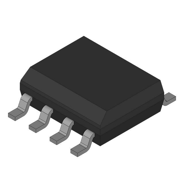
The Texas Instruments LM306D is a high-speed single differential voltage comparator with strobe control inputs and a push-pull output stage. The device is designed to convert small analog differential voltage variations into fast digital logic transitions and provides significantly faster response compared with general-purpose voltage comparators. The LM306D integrates a high-gain differential input stage, internal switching circuitry, two strobe control inputs, and a low-impedance push-pull output driver capable of high sink current. It operates from a dual supply configuration and is specified for commercial temperature operation from 0 °C to 70 °C. The device is available in an 8-pin SOIC package, with the LM306D designation representing the surface-mount version. The LM306 family is characterized by fast propagation delay, improved gain accuracy, TTL compatibility, strobe functionality, and output drive capability suitable for direct interface with digital logic systems.
## Device Architecture and Comparator Operating Principle
The LM306D is a high-speed differential comparator. Unlike an operational amplifier that is normally optimized for linear closed-loop amplification, a comparator is designed to operate primarily in open-loop mode and produce a digital output state according to the polarity of the differential input voltage.
The input stage consists of a differential amplifier configuration. The comparator continuously monitors the voltage difference between the non-inverting input and the inverting input. When the voltage at the non-inverting input exceeds the voltage at the inverting input, the internal switching circuitry drives the output toward the HIGH state. When the differential input voltage reverses polarity, the output transitions toward the LOW state.
The LM306D includes internal gain stages optimized for fast switching. The high open-loop gain allows the device to respond to small input voltage differences while maintaining rapid output transitions.
The device also integrates two strobe inputs. These inputs provide external control over comparator operation. When either strobe input is driven to a LOW logic level, the output is forced HIGH regardless of the differential input condition. When both strobe inputs are inactive or at a HIGH logic level, the output state is controlled normally by the differential input voltage.
## Supply Voltage and Electrical Operating Conditions
The LM306D is designed for operation with dual power supplies. The recommended supply configuration includes positive and negative supply rails, allowing the comparator input stage to process signals centered around ground potential.
The device operates with a positive supply voltage up to 24 V and supports negative supply operation from approximately -3 V to -12 V with minimal performance variation. The flexible negative supply range allows integration into various analog systems using different bipolar supply configurations.
The typical supply current is approximately 5.5 mA per channel. Since the LM306D contains a single comparator channel, this current represents the complete device operating current under specified conditions.
The operating temperature range is specified from 0 °C to 70 °C, corresponding to commercial-grade operation. Device performance parameters such as input offset voltage, propagation delay, and output characteristics are specified within this temperature range.
## Input Characteristics and Differential Performance
The LM306D uses a differential input structure capable of detecting relatively small voltage differences between the two input terminals.
The maximum input offset voltage is specified as 5 mV at 25 °C. Input offset voltage represents the differential input voltage required to force the comparator output into a defined switching condition when the two input terminals are nominally at the same voltage. Lower offset voltage improves threshold accuracy in voltage detection applications.
The maximum input bias current is specified at approximately 25 µA. This parameter represents the current required by the input transistor stage and must be considered when the comparator is connected to high-resistance signal sources or precision reference networks.
The input common-mode voltage range is specified between approximately 7 V and 17 V under the device operating conditions. The LM306D is not a rail-to-rail comparator, therefore input signals must remain within the specified common-mode voltage range to maintain proper operation.
## Propagation Delay and High-Speed Operation
A primary characteristic of the LM306D is its high-speed switching capability. The device provides a typical propagation delay time of approximately 28 ns, allowing it to respond rapidly to changing input conditions.
The short propagation delay results from optimized internal transistor stages designed specifically for comparator operation. Compared with general-purpose comparators intended for low-power applications, the LM306D provides significantly faster response characteristics.
Propagation delay is influenced by several factors, including input overdrive voltage, signal amplitude, supply voltage, temperature, and output loading conditions. Larger input differential voltages generally produce faster switching because the internal gain stages reach the switching threshold more quickly.
The high-speed characteristics make the LM306D suitable for applications requiring rapid analog-to-digital conversion, pulse detection, timing circuits, and fast control signal generation.
## Output Stage Characteristics
The LM306D incorporates a push-pull output stage rather than an open-collector output structure. This allows the device to actively drive both HIGH and LOW output states without requiring an external pull-up resistor.
The output stage is designed with low output impedance and high current capability. The device can provide output sink current up to approximately 100 mA, allowing direct drive of certain loads such as digital logic inputs, indicator devices, and control circuits.
The push-pull configuration improves switching speed because both output transitions are actively driven. The LOW-to-HIGH transition does not depend on an external resistor charging a capacitive load, as would occur in an open-collector comparator.
The high output drive capability allows the LM306D to interface directly with TTL logic systems. The device is specified to provide fanout capability for up to ten standard 54/74 series TTL loads.
## Strobe Function and Logic Control
The strobe function is a major feature of the LM306D architecture. The two strobe inputs allow external digital control of the comparator output independent of the analog input state.
When either strobe input is asserted LOW, the comparator output is forced HIGH. This effectively disables normal comparison operation and places the output into a controlled logic state.
When both strobe inputs are inactive, the comparator resumes normal operation, and the output is determined by the differential input voltage.
The strobe capability allows the LM306D to be used in systems requiring comparator enable control, signal gating, timing synchronization, and selective measurement functions.
The dual strobe inputs provide additional flexibility compared with standard comparators that only provide analog input and output terminals.
## Protection Features and Reliability
The LM306D incorporates internal protection functions designed to improve reliability during abnormal operating conditions.
The device includes short-circuit protection and surge-current limiting capability. These features help protect the output stage from excessive current conditions, although operation outside the absolute maximum ratings should still be avoided.
The protection circuitry limits damage caused by accidental output overload conditions. However, continuous operation under fault conditions may increase device temperature and reduce long-term reliability.
Proper power supply decoupling, appropriate input voltage control, and correct output loading are required to maintain stable operation.
## Package Characteristics
The LM306D is supplied in an 8-pin SOIC package. The package provides a compact surface-mount solution suitable for automated PCB assembly and space-constrained electronic designs.
The SOIC package offers reduced board area compared with traditional through-hole packages while maintaining compatibility with standard manufacturing processes.
Because the LM306D is a high-speed analog device, PCB layout has a direct influence on performance. Short signal paths, controlled grounding, and local supply bypass capacitors are important to minimize noise coupling and parasitic effects.
The package thermal characteristics must also be considered when operating the output stage near its maximum current capability.
## Application Areas
The LM306D is intended for applications requiring fast and accurate voltage comparison. Its high-speed response, strong output drive capability, and strobe control functions make it suitable for various analog and digital interface circuits.
Typical applications include high-speed threshold detection, zero-crossing detection, pulse generation, waveform shaping, analog-to-digital interface circuits, timing systems, and industrial control circuits.
The ability to directly drive TTL logic makes the device suitable for interfacing analog signal sources with digital processing systems.
The high output current capability also allows the comparator to directly control certain external loads without additional buffer stages, simplifying system design.
## Design Considerations
When implementing the LM306D, designers must consider input voltage range, supply configuration, output loading, and switching noise.
The input common-mode voltage must remain within the specified range because the device does not provide rail-to-rail input capability. Signals outside this range may cause incorrect switching behavior or degraded performance.
The output current capability should be evaluated carefully because high output current operation increases power dissipation and junction temperature.
High-speed comparator layouts require attention to signal integrity. Input traces should be protected from noise sources, and supply bypass capacitors should be located close to the device power pins.
The strobe inputs should be driven with clean digital signals to ensure predictable enable and disable behavior.
## Conclusion
The Texas Instruments LM306D is a high-speed differential comparator featuring fast response, push-pull output drive, dual strobe control inputs, and high-current output capability. It provides approximately 28 ns propagation delay, a 5 mV maximum input offset voltage at 25 °C, TTL-compatible output capability, and a low-impedance output stage capable of sinking up to 100 mA. The device operates in commercial temperature environments from 0 °C to 70 °C and is packaged in an 8-pin SOIC package. With its combination of high-speed comparison performance, programmable strobe control, and strong output drive capability, the LM306D is suitable for applications requiring rapid conversion of analog threshold information into digital control signals.