## Overview
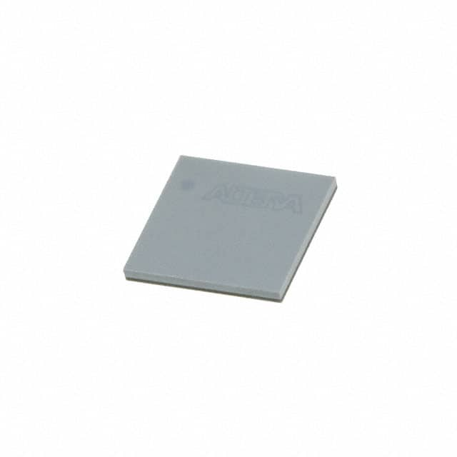
The Intel 10M02DCV36C8G is a member of the MAX 10 family of non-volatile Field-Programmable Gate Arrays (FPGAs), optimized for low- to mid-density applications that require low power, fast configuration, and high integration. The device integrates logic, embedded memory, analog-to-digital conversion, and configurable I/O in a single low-power FPGA, fabricated on a 55 nm process technology. It is suitable for industrial, consumer, and communications applications requiring deterministic performance, low cost, and high integration density.
## Architecture
* Technology: 55 nm low-power FPGA process
* Core Type: Non-volatile flash-based logic cells
* Logic Elements (LEs): 2,060
* Embedded Memory: 120 Kbits of MLABs and 240 Kbits of embedded M9K block RAM
* DSP Blocks: 8 9×9-bit multipliers for basic arithmetic operations
* Phase-Locked Loops (PLLs): 2 dedicated PLLs for clock management, multiplication, division, and deskewing
* I/O Pins: 36
* Package: 36-pin VQFN
* Speed Grade: -8 (fastest in the commercial range)
* Operating Temperature Range: 0°C to +85°C (commercial)
* Supports synchronous and asynchronous logic with deterministic timing for interface and control applications
* Non-volatile flash configuration provides instant-on operation without external configuration memory
This architecture allows low-power integration of logic, memory, analog, and digital peripherals in compact embedded systems.
## Logic Resources
* Total Logic Elements (LEs): 2,060
* Flip-Flops: Embedded within LEs for sequential logic
* Look-Up Tables (LUTs): 4-input per LE, supporting combinational and arithmetic functions
* Maximum Product Terms: Determined by LE configuration
* DSP Capabilities: 8 embedded 9×9 multipliers with optional add/subtract operations
* Embedded Memory: 120 Kbits of MLAB distributed RAM and 240 Kbits of dedicated M9K block RAM
* Supports implementation of finite-state machines, address decoding, arithmetic operations, and signal processing
* Deterministic propagation delays enable reliable multi-clock domain operation
## I/O Features
* Total I/O Pins: 36
* Supported I/O Standards: LVCMOS, LVTTL, SSTL, HSTL, and differential LVDS
* Input Voltage Thresholds: Configurable per I/O standard
* Output Drive: Programmable drive strength and slew rate
* Pin-to-Pin Propagation Delay: Typically 3–5 ns for standard LVCMOS I/O
* I/O Banks: Segmented to allow multiple voltage standards across different banks
* Flexible I/O configuration supports interfacing with microcontrollers, memory, sensors, ADC/DAC peripherals, and communication devices
## Timing Characteristics
* Maximum System Clock Frequency: 200 MHz for general-purpose logic paths
* Maximum DSP Clock Frequency: 250 MHz for arithmetic multipliers
* Embedded Memory Maximum Clock Frequency: 200 MHz
* Pin-to-Pin Propagation Delay: 3–5 ns typical
* Deterministic timing enables high-speed interface bridging, real-time control, and embedded signal processing
* Multi-clock domain designs supported with integrated PLLs and dedicated global clock networks
## Analog Features
* On-chip 12-bit ADC with up to 500 kS/s sampling rate
* Programmable input range: 0–1.8 V or 0–3.3 V depending on I/O bank
* Supports mixed-signal applications such as sensor interfacing, signal acquisition, and data logging
* Integrated reference voltage and input multiplexing reduce external component count
## Power Characteristics
* Core Voltage (VCCINT): 1.0 V typical
* I/O Voltage (VCCIO): 1.8 V to 3.3 V depending on I/O bank configuration
* Typical Power Consumption: 20–50 mW for moderate switching activity
* Maximum Power Consumption: Approximately 100 mW under full utilization
* Low static and dynamic power consumption optimized by flash-based architecture
* Supports power-saving modes, reducing consumption in idle or partial operation
## Package and Integration
* Package: 36-pin VQFN
* Small footprint suitable for space-constrained embedded systems
* Integrated logic, memory, DSP, and ADC reduce board-level component count
* Multi-voltage I/O banks enable interfacing with heterogeneous systems
* High integration allows compact design for low- to mid-density applications
## Applications
* Embedded control systems and finite-state machine logic
* Interface bridging and glue logic for industrial and consumer applications
* Data acquisition and sensor signal processing using integrated ADCs
* Low-power consumer and industrial electronics
* Communications and protocol bridging requiring moderate logic density and analog integration
## Development and Tool Support
* Supported by Intel Quartus Prime design software for design entry, synthesis, placement and routing, timing analysis, and programming
* JTAG interface available for in-system programming, functional verification, and debugging
* Predefined IP cores for memory controllers, DSP functions, ADC interfaces, and communication protocols
* Simulation and timing analysis tools enable verification of multi-clock designs and mixed-signal applications
* Flash-based non-volatile configuration ensures reliable instant-on operation and reduces board-level complexity
The Intel 10M02DCV36C8G is a low- to mid-density, low-power FPGA with integrated logic, memory, DSP, and ADC resources. Its flash-based non-volatile architecture, flexible I/O, and deterministic timing make it suitable for industrial, consumer, and embedded applications that require compact design, fast startup, and mixed-signal capabilities.