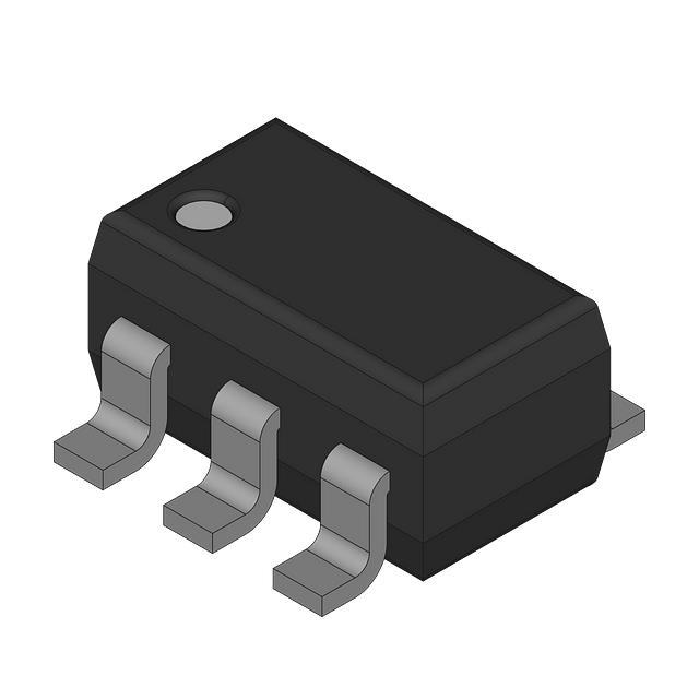
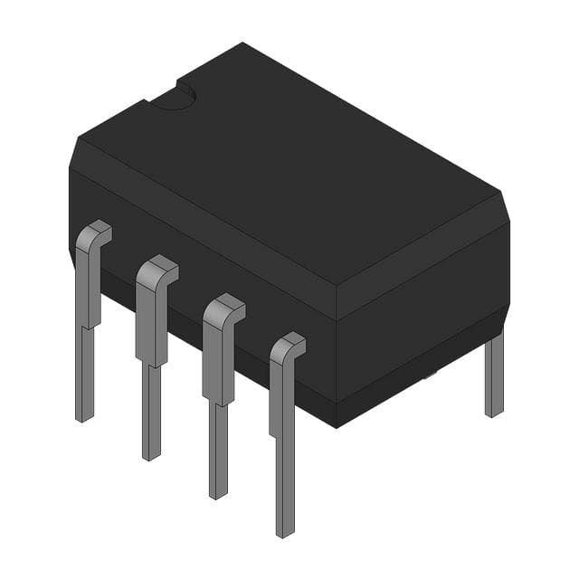
The Texas Instruments LMC6001BIN is a precision CMOS operational amplifier optimized for ultra-low input bias current, high input impedance, and low power consumption in high-impedance analog signal conditioning systems. It is designed for applications where picoampere-level input currents and minimal loading of sensor sources are critical, such as electrometer front ends, photodiode amplification, and precision instrumentation circuits. The device is supplied in an 8-pin PDIP package and belongs to the LMC6000 family, which is characterized by CMOS input architecture and rail-to-rail input capability within its specified common-mode range.
## Device Function and Technology Positioning
The LMC6001BIN is a single operational amplifier implemented using CMOS input transistor technology. Its primary design objective is minimizing input bias current while maintaining stable DC performance across temperature and supply variations.
Unlike bipolar-input operational amplifiers, the CMOS input stage eliminates base current-related offset errors, enabling ultra-high input impedance. This makes the device suitable for interfacing with high-impedance sources such as piezoelectric sensors, photodiodes, and electrochemical measurement systems.
The amplifier is optimized for low-frequency precision applications rather than high-speed signal processing. Its architecture prioritizes input leakage minimization and low power operation over high slew rate or wide bandwidth performance.
## Electrical Characteristics and Defined Parameters
The LMC6001BIN is characterized by extremely low input bias current, specified in the picoampere range under room temperature conditions. This parameter is one of the defining features of the device and directly impacts accuracy in high-impedance sensor circuits.
Input offset voltage defines the differential input voltage required to force the output to zero under specified conditions. This parameter is critical in precision DC measurement applications and is specified over temperature to ensure predictable behavior.
Supply voltage range defines the allowable operating window for single-supply or dual-supply operation. The device is designed for wide supply flexibility, supporting low-voltage operation while maintaining linear performance within its common-mode input range.
Input common-mode voltage range specifies the allowable voltage range over which the input stage remains linear and functional. The CMOS input structure enables operation close to supply rails under defined conditions, although output swing limitations must also be considered.
Output voltage swing defines how close the output can approach supply rails under specified load conditions. This is an important parameter in single-supply applications where maximum dynamic range is required.
Slew rate defines the maximum rate of change of output voltage over time. The LMC6001BIN is optimized for low-frequency precision operation, and its slew rate reflects this design focus rather than high-speed signal processing capability.
Gain bandwidth product (GBW) defines the frequency at which open-loop gain reduces to unity. This parameter determines the usable closed-loop bandwidth for stable amplifier configurations.
Open-loop gain defines the intrinsic amplification capability of the device under DC conditions. High open-loop gain is essential for precision amplification of small analog signals.
## Noise Performance and Signal Integrity
Input voltage noise density is specified for low-frequency operation and represents the intrinsic noise contribution of the amplifier. This parameter is critical in low-level signal amplification where microvolt-level signals are processed.
Current noise is extremely low due to CMOS input architecture, making the device suitable for high-source impedance applications where current noise would otherwise dominate signal degradation.
The combination of low bias current and low current noise makes the device particularly effective in high-impedance sensor front-end circuits, where leakage currents can significantly distort measurement accuracy.
## Power Consumption and Efficiency
The LMC6001BIN is designed for ultra-low power operation, with supply current significantly lower than bipolar operational amplifiers. This makes it suitable for battery-powered and long-duration sensing applications.
Power consumption scales linearly with supply voltage, enabling optimization for low-power embedded systems.
The CMOS architecture inherently reduces quiescent current consumption while maintaining stable DC performance across operating conditions.
## Input Protection and Reliability Characteristics
The input stage includes protection structures to prevent damage from electrostatic discharge and transient overvoltage conditions. These structures are designed to maintain ultra-low leakage characteristics while providing robustness in real-world environments.
Latch-up immunity is ensured through careful CMOS process design, preventing parasitic thyristor conduction under abnormal operating conditions.
Long-term stability is influenced by input protection leakage and package contamination sensitivity, particularly in ultra-high impedance applications where picoampere-level currents are measured.
## Package and Mechanical Characteristics
The LMC6001BIN is supplied in an 8-pin PDIP (plastic dual in-line package), which provides mechanical robustness and ease of prototyping and through-hole PCB assembly.
The package supports standard thermal dissipation for low-power analog circuits and provides sufficient isolation for high-impedance nodes when proper PCB layout techniques are used.
Pin configuration is standard for single operational amplifier devices, including non-inverting input, inverting input, output, and supply terminals.
## Typical Application Scenarios
The LMC6001BIN is primarily used in high-impedance signal conditioning applications where ultra-low input bias current is essential.
A key application is photodiode amplification circuits, where the amplifier converts extremely small photocurrents into measurable voltage signals without introducing significant leakage error.
It is also widely used in electrometer-grade measurement systems, including ion sensors, pH measurement circuits, and other electrochemical sensing applications.
Additional applications include charge amplifiers for piezoelectric sensors, long-duration integrator circuits, and precision instrumentation front ends where DC accuracy is more critical than bandwidth.
The device is not intended for high-speed signal processing, audio power amplification, or high-drive output stages due to its low slew rate and limited output drive capability.
## System-Level Design Considerations
PCB layout is critical in maintaining ultra-high input impedance performance. Surface contamination, flux residues, and leakage paths across the PCB can significantly degrade measurement accuracy at picoampere input current levels.
Guarding techniques are often required around high-impedance input nodes to minimize leakage currents and parasitic conduction paths.
Power supply decoupling must be implemented close to the device pins to ensure stable operation and minimize noise coupling into the analog signal path.
Feedback network design must consider resistor leakage and thermal noise contributions, as external components can dominate system-level accuracy rather than the amplifier itself.
## Conclusion
The Texas Instruments LMC6001BIN is an ultra-low input bias current CMOS operational amplifier optimized for high-impedance precision analog applications requiring picoampere-level input leakage, low power consumption, and stable DC performance. Its CMOS input architecture, low noise characteristics, and high input impedance make it suitable for electrometer-grade sensing and photodiode amplification systems, provided that PCB leakage control, guarding techniques, and precision passive component selection are carefully implemented at system level.