Overview of Texas Instruments ADCS7477AIMF/NOPB
The Texas Instruments ADCS7477AIMF/NOPB is a high-speed, 12-bit analog-to-digital converter (ADC) designed for a wide range of precision data acquisition and signal processing applications. It features a low-power successive approximation register (SAR) architecture that delivers fast conversion times combined with excellent dynamic performance. This ADC is targeted for use in industrial automation, instrumentation, communications, and medical equipment, where accurate digitization of analog signals is critical.
Key Features
* 12-bit resolution with high linearity and accuracy
* Maximum sampling rate of up to 1 MSPS (mega-samples per second)
* Low power consumption suitable for portable and battery-powered systems
* Single-ended input with unipolar input voltage range from 0 V to reference voltage (typically 5 V)
* Serial peripheral interface (SPI) compatible digital output for easy microcontroller and DSP integration
* Wide power supply voltage range from 4.5 V to 5.5 V
* Internal sample-and-hold amplifier for accurate acquisition of fast-changing signals
* Low total harmonic distortion (THD) and excellent signal-to-noise ratio (SNR)
* No pipeline delay and latency-free output for real-time applications
* Pin-compatible with many similar 12-bit SAR ADCs facilitating easy upgrades
* Lead-free, RoHS-compliant package suitable for environmental standards
Electrical Specifications
* Resolution: 12 bits
* Sampling Rate: Up to 1 MSPS
* Input Voltage Range: 0 V to VREF (typically 5 V) single-ended input
* Integral Nonlinearity (INL): ±1 LSB maximum
* Differential Nonlinearity (DNL): ±0.5 LSB typical, ±1 LSB maximum
* Signal-to-Noise Ratio (SNR): Approximately 68 dB at 1 MSPS
* Spurious-Free Dynamic Range (SFDR): Greater than 80 dB
* Total Harmonic Distortion (THD): Typically –80 dB at 1 kHz input
* Power Supply Voltage: 4.5 V to 5.5 V
* Power Dissipation: Approximately 20 mW at 1 MSPS
* Input Capacitance: 7 pF typical
* Operating Temperature Range: –40°C to +85°C (Industrial grade)
* Reference Input: External reference voltage input, typically 5 V
Functional Description
The ADCS7477AIMF/NOPB uses a successive approximation register architecture to convert an analog input signal to a 12-bit digital output word. The device includes an internal track-and-hold amplifier which accurately captures the input voltage during the acquisition phase, enabling fast and precise sampling of signals with rapid changes.
The digital interface employs a standard SPI-compatible serial protocol with a four-wire interface (clock, chip select, data in, and data out) allowing seamless connection to microcontrollers, digital signal processors, or FPGAs. This interface supports continuous conversion mode, maximizing throughput for real-time data acquisition systems.
The converter’s performance is enhanced by low noise and distortion characteristics, making it suitable for precision instrumentation where signal fidelity is paramount. Additionally, the device features a power-down mode to reduce consumption during idle periods, aiding energy-efficient system designs.
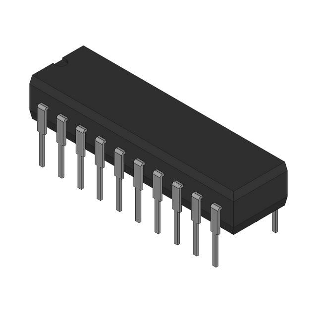
Package and Pin Configuration
The ADCS7477AIMF/NOPB is offered in a compact 28-pin thin shrink small-outline package (TSSOP) with a lead-free RoHS-compliant design. The pinout includes:
* Analog input pin
* Reference voltage input pin
* SPI digital interface pins (SCLK, SDI, SDO, CS)
* Power supply and ground pins
* Power-down and conversion control pins
The TSSOP package allows for dense PCB layouts suitable for modern industrial and consumer electronic products.
Applications
* Industrial process control and automation requiring high-speed, accurate measurement
* Data acquisition systems for scientific instrumentation and test equipment
* Communications systems for digitizing analog signals with high fidelity
* Medical imaging and diagnostic devices needing precise and fast analog-to-digital conversion
* Motor control and power electronics monitoring
* Battery-powered portable instruments demanding low power and high resolution
Performance and Design Considerations
The device’s high sample rate of 1 MSPS enables it to capture fast transient signals, while the 12-bit resolution ensures precise digital representation. However, designers must carefully manage layout to minimize analog noise coupling into the ADC input, and choose an accurate, low-noise reference voltage source to maximize conversion accuracy.
The SPI interface’s timing requirements must be respected to ensure data integrity, especially at high conversion rates. Power supply decoupling and careful grounding are essential to maintain optimal performance.
Reliability and Environmental Specifications
The ADCS7477AIMF/NOPB is rated for industrial temperature ranges (–40°C to +85°C), ensuring stable operation in harsh environments. The package and manufacturing processes meet environmental compliance standards, including lead-free and RoHS requirements, making it suitable for global markets.
---
If you want, I can also provide example interfacing circuits or performance graphs for the ADCS7477AIMF/NOPB. Would you be interested in that?