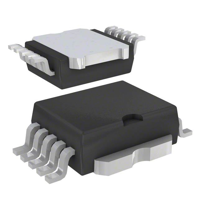
The STMicroelectronics VND830MSP13TR is a monolithic high-side driver integrated circuit based on ST’s VIPower M0-3 technology, designed for automotive-grade power switching applications. It integrates a power MOSFET with dedicated gate driving, diagnostic, and protection circuitry, enabling direct control of inductive, resistive, and capacitive loads in 12 V automotive electrical systems. The device is optimized for robust load switching with built-in protection against overcurrent, overtemperature, and short-circuit conditions, making it suitable for body electronics and power distribution modules.
## Device Function and Architectural Positioning
The VND830MSP13TR is a dual-channel high-side power switch IC intended to drive automotive loads from the positive supply rail. Each channel integrates a power MOSFET that connects the load to the supply voltage when activated via a logic-level input signal.
The device belongs to STMicroelectronics VIPower family, which combines vertical power MOSFET technology with logic-level control and diagnostic functions in a single silicon die. This integration eliminates the need for external gate drivers, current sensing resistors, and discrete protection components.
The primary function is controlled high-side switching of automotive loads such as lamps, motors, solenoids, and heating elements, with additional diagnostic feedback capability for system monitoring.
## Device Identification and Package Characteristics
The part number VND830MSP13TR identifies a dual-channel VIPower high-side driver in the VND family. The “VND” prefix indicates VIPower automotive power switch technology. The “830” denotes the specific dual-channel configuration and current capability class within the family.
The “MSP” suffix indicates a MultiPowerSO package variant optimized for high thermal performance and compact PCB integration. The “13” refers to a specific internal configuration or revision level within the device family, and “TR” denotes tape-and-reel packaging for automated SMT assembly.
The MultiPowerSO package integrates exposed thermal pads to ensure efficient heat dissipation from the power MOSFET die to the PCB copper plane, which is critical for sustained high-current operation.
## Power Switching Architecture and Operation Principle
The VND830MSP13TR integrates two independent high-side N-channel power MOSFETs, each controlled by a corresponding logic input. When a logic high signal is applied to the input pin, the internal driver circuitry enhances the MOSFET gate voltage, enabling current flow from the supply to the load.
The high-side configuration ensures that the load remains referenced to ground while switching the positive supply rail, which is standard in automotive electrical architectures.
The integrated structure includes level shifting circuitry to allow low-voltage logic signals (typically microcontroller-compatible) to control high-voltage power switching stages.
## Electrical Characteristics and Operating Parameters
The device is designed for operation in 12 V automotive systems, with extended tolerance for load dump and transient conditions typical in vehicle electrical environments.
Each channel incorporates a low on-state resistance power MOSFET, which determines conduction losses and thermal dissipation under load current conditions. The RDS(on) parameter is a critical performance metric, directly affecting voltage drop and power efficiency.
The device supports continuous load current per channel within specified thermal limits, with peak current capability dependent on pulse duration and thermal impedance conditions.
Input logic thresholds are compatible with standard CMOS/TTL-level control signals, allowing direct interface with microcontrollers and automotive control units.
## Protection Mechanisms and Diagnostic Functions
The VND830MSP13TR integrates multiple protection features essential for automotive reliability:
Overcurrent protection limits output current in the event of load short-circuit conditions. The device transitions into a current-limiting mode to prevent catastrophic failure of the internal MOSFET.
Thermal shutdown protection disables the output stage when junction temperature exceeds a predefined threshold. The device automatically recovers once temperature returns to a safe operating range.
Short-circuit protection is implemented through active current sensing within the power MOSFET structure, eliminating the need for external sense resistors.
Diagnostic feedback is provided via status output pins, enabling detection of open-load conditions, short-to-ground, and short-to-supply faults depending on operating state.
## Switching Behavior and Dynamic Performance
The device is designed for controlled switching of inductive and resistive loads. Turn-on and turn-off transitions are internally managed to reduce electromagnetic interference (EMI) and limit voltage overshoot caused by inductive load switching.
For inductive loads such as solenoids and relays, internal clamp structures provide energy dissipation paths to protect the MOSFET from voltage transients generated during turn-off events.
The switching speed is optimized to balance thermal stress, EMI performance, and switching efficiency in automotive environments.
## Thermal Management and Power Dissipation
Thermal performance is a critical design parameter for the VND830MSP13TR. Power dissipation occurs primarily in the MOSFET conduction path, proportional to load current and RDS(on).
The MultiPowerSO package provides a low thermal resistance path from silicon junction to PCB, enabling efficient heat spreading. Proper PCB copper area and thermal vias are required to achieve rated current performance.
Thermal shutdown protection ensures safe operation under overload or high ambient temperature conditions, preventing permanent damage.
## Package and Mechanical Characteristics
The device is housed in a MultiPowerSO surface-mount package designed specifically for automotive power applications. The package includes exposed thermal pads and wide lead frames to support high current density and efficient heat transfer.
The mechanical structure is optimized for vibration resistance and long-term reliability under automotive environmental conditions, including temperature cycling and mechanical stress.
The tape-and-reel (TR) format supports automated high-volume PCB assembly processes used in automotive manufacturing.
## System-Level Application Context
The VND830MSP13TR is used in automotive body control systems for switching and driving a wide range of loads. Typical applications include lamp control (headlamps, tail lamps, interior lighting), solenoid actuation, relay driving, and motor control in low-to-medium power subsystems.
It is commonly integrated into body control modules (BCM), fuse replacement electronic modules, and distributed power control architectures where electronic switching replaces mechanical relays.
The integrated diagnostics and protection features make it suitable for safety-critical automotive subsystems requiring fault detection and system-level monitoring.
## Conclusion
The STMicroelectronics VND830MSP13TR is a dual-channel VIPower high-side driver IC integrating power MOSFETs, control logic, protection circuits, and diagnostic functionality in a thermally enhanced MultiPowerSO package. Designed for automotive 12 V systems, it provides robust load switching capability with integrated current limiting, thermal protection, and fault diagnostics. Its monolithic architecture enables reliable and compact replacement of discrete relay-based switching solutions in modern automotive power distribution and body electronics systems.