The Infineon Technologies BF2030WH6824XTMA1 is a silicon N-channel RF MOSFET tetrode optimized for low-noise and high-gain amplification in VHF and UHF front-end applications. The device is specifically designed for RF signal amplification stages in television tuners, antenna amplifiers, communication receivers, broadband RF modules, and other high-frequency analog circuits operating up to approximately 1 GHz. It combines low noise figure, high transconductance, stable RF behavior, and compact surface-mount packaging, making it suitable for modern high-density RF systems where signal integrity and low power consumption are critical design priorities.
The device belongs to Infineon’s RF small-signal MOSFET portfolio and is manufactured using optimized silicon MOS technology intended for high-frequency operation. Compared with conventional bipolar RF transistors, the BF2030 architecture provides improved gain control capability, lower reverse transfer capacitance, enhanced input impedance characteristics, and simplified biasing requirements. These properties allow the transistor to achieve stable low-noise operation across a wide frequency range while maintaining efficient RF amplification performance.
## Device Structure and Technology
The BF2030WH6824XTMA1 utilizes an N-channel MOSFET tetrode structure. In RF electronics, tetrode MOSFET configurations are particularly valuable because they allow improved isolation between input and output sections while supporting gain control functionality. The device incorporates multiple gate regions that reduce unwanted feedback capacitance and improve high-frequency stability.
The MOSFET channel geometry is optimized for low intrinsic noise generation and high transconductance at relatively low drain currents. This enables the device to amplify weak RF signals efficiently without introducing excessive thermal or flicker noise into the receiver chain. Because the first amplification stage largely determines the overall system noise figure, low-noise RF MOSFETs such as the BF2030 are commonly used at antenna interfaces and tuner front ends.
The transistor is fabricated using planar silicon processing technology optimized for RF small-signal applications. The process minimizes parasitic capacitances and improves frequency response while maintaining reliable operation under standard commercial and industrial environmental conditions.
## Package Information
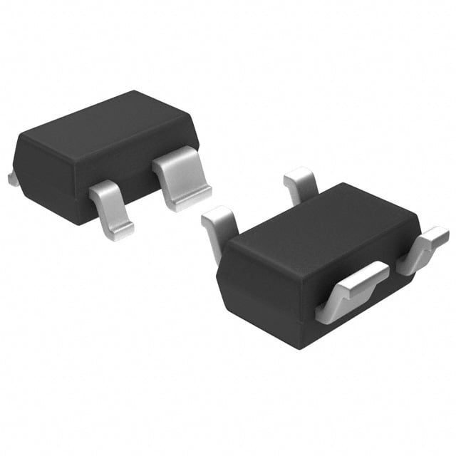
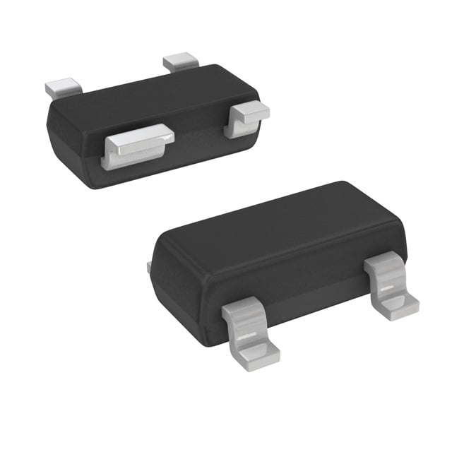
The BF2030WH6824XTMA1 is supplied in the compact PG-SOT343 package, also referenced as SC-82A. This miniature four-lead surface-mount package is specifically intended for high-density PCB layouts and automated assembly processes.
Key package characteristics include:
* Package type: PG-SOT343-4
* Alternative package designation: SC-82A
* Mounting technology: Surface mount
* Terminal count: 4 leads
* Packaging format: Tape and reel
* Pb-free and RoHS compliant construction
* Moisture Sensitivity Level: MSL1
The extremely small package footprint minimizes parasitic inductance and capacitance, both of which are critical parameters in RF circuit design. Reduced parasitic elements help maintain gain consistency and stable impedance characteristics at frequencies approaching 1 GHz.
The package also supports automated high-speed SMT production, making the device suitable for large-scale consumer electronics manufacturing and compact RF module integration.
## Electrical Specifications
The BF2030WH6824XTMA1 is designed for low-voltage RF amplification applications. Typical electrical parameters include:
* Transistor polarity: N-channel
* Technology: RF MOSFET tetrode
* Maximum drain-source voltage (VDS): approximately 8 V
* Typical operating drain voltage: 5 V
* Drain current capability: approximately 40 mA
* Typical operating drain current: approximately 10 mA
* Typical gain: approximately 23 dB
* Typical noise figure: approximately 1.5 dB
* Frequency capability: operation extending toward 1 GHz
* Low reverse transfer capacitance
* High transconductance optimized for RF gain stages
The low operating voltage allows integration into low-power RF systems and battery-powered communication equipment. In addition, the relatively low drain current minimizes thermal dissipation while still providing sufficient gain for front-end signal conditioning.
The gain characteristic of approximately 23 dB enables substantial signal amplification in a single stage, which can reduce overall component count and simplify RF amplifier topology.
## Noise Performance
Noise figure is one of the most important parameters for RF front-end devices, especially in weak-signal reception systems. The BF2030WH6824XTMA1 achieves a typical noise figure near 1.5 dB, allowing excellent receiver sensitivity in broadband communication and tuner applications.
Low-noise operation is achieved through optimized MOSFET channel design and minimized gate leakage currents. The MOS structure inherently provides high input impedance, which helps reduce signal loading effects at the antenna interface.
In practical RF systems, the BF2030 can be used in:
* Antenna preamplifiers
* Television tuner inputs
* VHF/UHF receiver front ends
* Satellite signal conditioning circuits
* RF instrumentation amplifiers
* Broadband low-noise amplifiers
The low-noise characteristics are especially important because the first RF stage dominates the total cascaded system noise figure according to Friis noise theory. Therefore, using a low-noise MOSFET significantly improves overall receiver performance.
## RF Gain Characteristics
The device provides high RF gain while maintaining stable operation across a wide frequency spectrum. High transconductance enables efficient conversion of small input voltage variations into amplified drain current signals.
The relatively low gate-drain capacitance contributes to:
* Reduced feedback effects
* Improved amplifier stability
* Lower oscillation tendency
* Better high-frequency isolation
* Simplified impedance matching
At UHF frequencies, even small parasitic capacitances can negatively affect gain and stability. The BF2030’s optimized internal structure and compact package help mitigate these issues.
The transistor is particularly suitable for broadband amplification stages where flat frequency response and stable gain are required across wide operating bands.
## Gain Control Capability
One major advantage of RF MOSFET tetrode devices is controlled gain functionality. By adjusting gate bias conditions, designers can dynamically regulate amplifier transconductance and overall signal gain.
This capability is useful in:
* Automatic gain control systems
* Signal leveling circuits
* Adaptive receiver architectures
* Variable sensitivity tuner modules
* Dynamic range optimization stages
In communication receivers, AGC operation prevents overload from strong incoming signals while still allowing amplification of weak signals. The BF2030 supports this functionality through its MOSFET gate control characteristics.
Compared with fixed-gain bipolar transistor stages, MOSFET tetrode architectures offer improved flexibility in variable-gain RF applications.
## Frequency Response and Stability
The BF2030WH6824XTMA1 is optimized for VHF and UHF operation, with usable frequency response extending close to 1 GHz. High-frequency operation requires careful management of parasitic inductance, interelectrode capacitance, and PCB layout geometry.
The transistor demonstrates good RF stability because of:
* Low internal capacitance
* Compact lead structure
* Reduced feedback coupling
* Optimized RF silicon process
* Stable transconductance characteristics
These properties allow the device to operate reliably in tuned amplifier circuits and broadband RF front ends without excessive compensation requirements.
For frequencies approaching the upper operating range, PCB transmission-line effects become increasingly important. Designers commonly use controlled-impedance traces, solid RF grounding, and carefully optimized matching networks to achieve maximum performance.
## Thermal Characteristics
The BF2030 is a low-power RF transistor and therefore exhibits relatively modest thermal dissipation requirements compared with power RF MOSFETs. Nevertheless, proper thermal design remains important for maintaining long-term stability and minimizing parameter drift.
Thermal considerations include:
* Proper copper grounding area beneath the package
* Short thermal conduction paths
* Adequate airflow in dense RF modules
* Minimization of localized hot spots
* Stable bias current management
The low operating current reduces self-heating effects, which contributes to stable noise figure and gain characteristics over temperature variation.
Because RF transistor performance can shift with junction temperature, maintaining good thermal stability improves frequency response consistency and reduces long-term degradation.
## PCB Design Recommendations
Successful implementation of the BF2030WH6824XTMA1 requires careful RF PCB layout practices. At VHF and UHF frequencies, PCB parasitics significantly influence overall circuit behavior.
Recommended layout techniques include:
* Minimize RF trace lengths
* Use continuous low-impedance ground planes
* Place decoupling capacitors close to supply nodes
* Maintain physical separation between input and output sections
* Use controlled-impedance RF traces where necessary
* Reduce loop inductance in grounding paths
Input and output matching networks should be optimized for the intended operating frequency range. Small variations in layout geometry can substantially affect gain, noise figure, and stability at high frequencies.
The compact SOT343 package helps reduce parasitic inductance, simplifying high-frequency PCB integration compared with larger leaded packages.
## Typical Applications
The BF2030WH6824XTMA1 is widely applicable in low-noise RF amplification systems. Common applications include:
* Television tuner front ends
* Broadband antenna amplifiers
* VHF communication receivers
* UHF signal boosters
* RF preamplifiers
* Wireless receiver modules
* FM radio front-end stages
* Satellite receiver input circuits
* Industrial RF instrumentation
* Scanner receiver front ends
Its low-voltage operation also makes it suitable for portable communication equipment and compact embedded RF modules where power efficiency is important.
## Advantages in RF System Design
The BF2030 offers several important advantages in practical RF circuit implementation:
* Low noise figure for improved receiver sensitivity
* High gain at VHF and UHF frequencies
* Compact surface-mount package
* Low operating voltage and power consumption
* Good gain control characteristics
* Reduced feedback capacitance
* High-frequency operational stability
* Simplified RF front-end design
These characteristics make the device particularly attractive for compact tuner systems and broadband communication equipment requiring stable low-noise amplification.