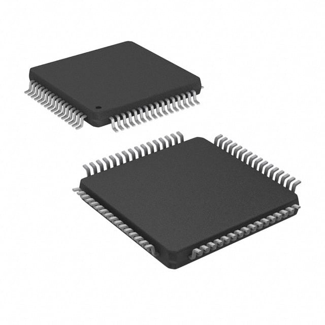
The CLC030VEC is a high-speed serial link transmitter device from Texas Instruments designed for short-reach digital video and data transmission applications over coaxial cable or controlled impedance transmission media. It is part of TI’s Channel Link architecture family, which implements parallel-to-serial conversion to reduce interconnect complexity while maintaining high aggregate data throughput. The device is optimized for compact board-level integration in systems requiring deterministic high-speed digital data transport with reduced pin count interconnects.
## Device Function and Architectural Positioning
The CLC030VEC is a serializer integrated circuit that converts a wide parallel CMOS/LVTTL-compatible input bus into a high-speed serial data stream. Its primary function is to reduce the number of physical interconnect lines required between a source device (such as an image sensor, video processing ASIC, or FPGA) and a remote receiver by encoding parallel data into a serialized high-frequency bitstream.
The device belongs to the Channel Link family, which is architected around source-synchronous serialization. In this architecture, data is captured synchronously with an input clock, serialized internally, and transmitted over a single differential or single-ended high-speed output channel depending on system configuration.
The CLC030VEC is designed for deterministic latency operation, meaning that the serialization process introduces a fixed and predictable delay between input and output domains. This property is critical in video transport systems where timing alignment between pixel clocks and data streams must be preserved.
## Input Interface and Parallel Data Handling
The device accepts a multi-bit parallel input data bus operating in synchronization with an external clock signal. The input interface is designed for compatibility with standard CMOS logic levels used in FPGA and ASIC environments.
Data is sampled on clock edges and buffered internally before serialization. The architecture ensures that each input word is mapped deterministically into a serialized bit sequence. This mapping preserves word alignment and ensures that the receiver can reconstruct the original parallel data stream without ambiguity.
The input clock serves as the reference for serialization timing. This clock is internally multiplied or phase-locked depending on the internal serialization ratio, which is fixed by device architecture and Channel Link protocol design.
## Serialization Architecture and High-Speed Output
At the core of the CLC030VEC is a high-speed shift register-based serializer operating at a multiple of the input clock frequency. The device converts each parallel input word into a continuous serial bitstream transmitted at a significantly higher bit rate than the input clock frequency.
The serialized output is designed for transmission over controlled impedance media, typically including coaxial cables or differential transmission lines. The output stage is engineered to maintain signal integrity at high switching speeds, with controlled edge rates to minimize electromagnetic interference and signal reflections.
The serialization process is deterministic and frame-aligned, ensuring that the receiver can recover word boundaries using embedded or accompanying clocking mechanisms provided by the Channel Link ecosystem.
## Clocking and Timing Architecture
The CLC030VEC relies on a source-synchronous clocking architecture. The input clock is used both for data capture and as a timing reference for serialization. The device generates a corresponding high-speed clocking relationship between serialized data and the associated timing signal required for downstream deserialization.
Timing alignment between data and clock is a critical design parameter. The device ensures that setup and hold time requirements are maintained at the input interface, while output timing skew is minimized through internal clock distribution optimization.
The system is designed to support predictable propagation delay, enabling deterministic timing closure in high-speed serial link designs.
## Electrical Interface Characteristics
The input interface of the CLC030VEC is CMOS-compatible and designed to interface directly with logic-level digital systems. Input thresholds are defined to ensure compatibility with standard digital logic families used in embedded video processing systems.
The output interface is a high-speed serial driver designed to operate into controlled impedance transmission lines. The output stage is optimized for signal integrity over short-to-medium reach interconnects, typically board-to-board or chassis-level cabling.
Signal integrity considerations include controlled output slew rate, impedance matching, and minimized jitter contribution from the serialization logic. These parameters are essential for maintaining eye diagram integrity at the receiver end.
## Functional Integration and System-Level Behavior
The device is typically used as part of a transmitter-receiver pair within the Channel Link architecture. In such configurations, the CLC030VEC operates as the serialization front-end, while a complementary deserializer reconstructs the original parallel data stream at the receiving end.
System-level operation is based on maintaining synchronization between transmitter and receiver clocks. The serialized data stream carries sufficient timing information to allow the receiver to recover the original data phase relationship.
The architecture is designed for continuous streaming operation rather than packetized communication, making it suitable for real-time video and deterministic data transfer systems.
## Power Supply and Electrical Operating Conditions
The CLC030VEC operates from a single supply rail consistent with high-speed CMOS serialization devices. Internal circuitry includes high-speed digital logic blocks and output drivers optimized for low jitter and controlled switching behavior.
Power consumption is primarily dependent on switching activity within the serializer and output driver load conditions. Dynamic power dissipation scales with data transition density and output switching frequency.
Proper decoupling and PCB layout practices are required to maintain signal integrity and minimize supply noise coupling into high-speed internal nodes.
## Package and Physical Implementation
The device is provided in a high-density surface-mount package intended for compact PCB layouts in high-speed digital systems. The package is optimized for minimizing parasitic inductance and capacitance, which is critical for preserving signal integrity at multi-hundred megabit per second serialization rates.
Thermal dissipation requirements are moderate compared to high-power analog devices but must be considered in dense multi-channel video systems where multiple serializers may operate simultaneously.
## Typical Application Scenarios
The CLC030VEC is primarily used in high-speed digital video transmission systems, including industrial imaging, machine vision, and embedded display systems. It is also applicable in FPGA-to-display or sensor-to-processing unit interconnects where parallel bus reduction is required.
Additional use cases include board-level interconnect reduction in systems with constrained PCB routing resources, where replacing wide parallel buses with serialized links reduces routing complexity and improves signal integrity.
The device is particularly effective in applications requiring deterministic latency and continuous real-time data streaming, such as frame-based imaging pipelines and synchronized multi-channel acquisition systems.
## Conclusion
The CLC030VEC is a high-speed Channel Link serializer designed to convert wide parallel digital data buses into a deterministic high-frequency serial data stream. Its architecture is centered on source-synchronous timing, fixed-latency serialization, and controlled impedance high-speed output signaling. The device enables significant interconnect reduction in high-throughput digital systems while preserving timing integrity and data determinism, making it suitable for real-time video transport and high-speed embedded digital communication architectures.